
Simulation and Comparative Study of Resonant Tunneling Diode
DOI:
https://doi.org/10.48048/tis.2022.5615Keywords:
Resonant tunneling diode, Double barrier, Triple barrier, Six barrierAbstract
This paper studies and investigates the effect of physical and electrical parameters on double, triple and six barrier resonant tunneling diodes (RTD). The materials used for quantum well and barriers are Gallium arsenide (GaAs) and Aluminium gallium arsenide (AlGaAs), respectively. The parameters that were reasoned and studied include conduction band, current density, transmission coefficient and resonance energy. The above parameters were studied by changing bias voltage, temperature, barrier width and doping concentration. From the simulations performed it is observed that for double barrier RTD the peak current density is observed at 0.2 V and the valley current density is observed at 0.3 V, whereas for a triple barrier RTD the peak current density is observed at 0.015 V and the valley current density is observed at 0.06 V. The value of transmission coefficient for double barrier RTD decreases especially after bias applied is more than resonant bias (0.2 V). The effect of increasing bias leads to a decrease in the resonance level in the conduction band. The width of resonance energy decreases with the increase in barrier width. With increase in number of barrier the number of resonance level increases which leads to an increasing peaks in the transmission coefficient curve. The effect of increasing temperature leads to higher current and more resonance energy. With the thickening of barrier width, less transmission of electrons occurs leading to a reduced current density. When the barriers are increased the negative differential region (NDR) is achieved at low voltages.
HIGHLIGHTS
- This paper studies and investigates the effect of physical and electrical parameters on double, triple and six barrier resonant tunneling diodes (RTD)
- The parameters include conduction band, current density, transmission coefficient, and resonance energy
- The parameters were studied by changing bias voltage, temperature, barrier width, and doping concentration
- It is observed that for double barrier RTD the peak current density is observed at 0.2 V and the valley current density is observed at 0.3 V
- For a triple barrier RTD the peak current density is observed at 0.015 V and the valley current density is observed at 0.06 V
GRAPHICAL ABSTRACT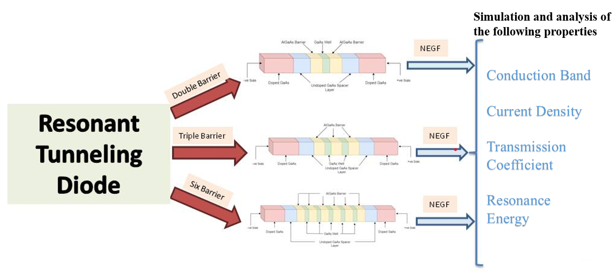
Downloads
References
H Mizuta and T Tanoue. The physics and applications of resonant tunnelling diodes. Vol II. Cambridge University Press, Cambridge, 2006.
S Saha, K Biswas and MR Hossain. Analysis of digital inverter using single and multiple GaAs/AlGaAs based double barrier resonant tunneling diode. In: Proceedings of the International Conference on Innovation in Engineering and Technology, Dhaka, Bangladesh. 2018, p. 1-6.
J Lee, J Lee and K Yang. A low-power 40-Gb/s 1:2 demultiplexer IC based on a resonant tunneling diode. IEEE Trans. Nanotechnol. 2012; 11, 431-4.
SF Nafea and AAS Dessouki. An accurate large-signal SPICE model for resonant tunneling diode. In: Proceedings of the International Conference on Microelectronics, Cairo, Egypt. 2010, p. 507-10.
AL Elgreatly, AA Shaaban and ESM El-Rabaie. Enhancement of drams performance using resonant tunneling diode buffer. In: Proceedings of the 1st International Conference on Information Technology, Computer and Electrical Engineering, Semarang, Indonesia. 2014, p. 16-20.
M Asada and S Suzuki. Terahertz emitter using resonant-tunneling diode and applications. Sensors 2021, 21, 1384.
M Reddy. 1997, Schottky-collector resonant tunnel diodes for sub-millimeter-wave applications. Ph. D. Dissertation. University of California, Santa Barbara, California.
TJ Slight and CN Ironside. Investigation into the integration of a resonant tunnelling diode and an optical communications laser: Model and experiment. IEEE J. Quant. Electron. 2007; 43, 580-7.
S Lin, DWang, Y Tong, B Shen and X Wang. III-nitrides based resonant tunneling diodes. J. Phys. D Appl. Phys. 2020; 53, 253002.
LL Chang, EE Mendez and C Tejedor. Resonant tunneling in semiconductors physics and applications. Plenum Press, New York, 1991.
TCLG Sollner, WD Goodhue, PE Tannenwald, CD Parker and DD Peck. Resonant tunneling through quantum wells at frequencies up to 2.5 THz. Appl. Phys. Lett. 1983; 42, 588.
H Yamamoto, Y Kanie, M Arakawa and K Taniguchi. Theoretical study of resonant tunneling in rectangular double-, triple-, quadruple-, and quintuple-barrier structure. Appl. Phys. A 1990; 50, 577-81.
VN Do, P Dollfus and V Lien Nguyen. Transport and noise in resonant tunneling diode using self-consistent Green’s function calculation. J. Appl. Phys. 2006; 100, 093705.
G Klimeck. Tutorial 4a: High bias quantum transport in resonant tunneling diodes, Available at: https://nanohub.org/resources/11043, accessed January 2021.
MM Singh, MJ Siddiqui, AB Khan and SG Anjum. Effect of barriers length and doping concentration on GaAs/AlGaAs RTD. In: Proceedings of the Annual IEEE India Conference, New Delhi, India. 2015.
T Rong, LA Yang, Z Zhao, K Zhang and Y Hao. Theoretical modeling of triple‐barrier resonant‐tunneling diodes based on AlGaN/GaN heterostructures. Phys. Status Solidi A 2019; 216, 1900471.
WNN Zaharim, NZI Hashim, MFP Mohamed, AA Manaf and MAM Zawawi. Physical modelling of gallium nitride (GaN) based double barrier quantum well device. In: M Zawawi, S Teoh, N Abdullah, MM Sazali (Eds.). Lecture notes in electrical engineering. Vol 547. Springer, Singapor, 2019, p. 141-8.
S Almansour and H Dakhlaoui. Electromodulation of the negative differential resistance in an AlGaAs/GaAs resonant tunneling diode. J. Korean Phys. Soc. 2019; 74, 36-40.
S Almansour. Theoretical study of electronic properties of resonant tunneling diodes based on double and triple AlGaAs barriers. Results Phys. 2020; 17, 103089.
EDG Castro, F Rothmayr, S Krüger, G Knebl, A Schade, J Koeth, L Worschech, V Lopez-Richard, GE Marques, F Hartmann, A Pfenning and S Höfling. Resonant tunneling of electrons in AlSb/GaInAsSb double barrier quantum wells. AIP Adv. 2020; 10, 055024.
S Sawai and K Narahara. Submillimeter-wave multiphase oscillation using traveling pulses in a resonant-tunneling diode-oscillator lattice. J. Infrared Millimet. Terahertz Waves 2021; 42, 426-45.
Y Nishida, N Nishigami, S Diebold, J Kim, M Fujita and T Nagatsuma. Terahertz coherent receiver using a single resonant tunnelling diode. Sci. Rep. 2019; 9, 18125.
LL Chang, L Esaki and R Tsu. Resonant tunneling in semiconductor double barriers. Appl. Phys. Lett. 1974; 24, 593.
S Datta. Nanoscale device modeling: The Green’s function method. Superlattice. Microst. 2000; 28, 253-78.
S Datta. The non-equilibrium Green’s function (NEGF) formalism: An elementary introduction. In: Proceedings of the Digest. International Electron Devices Meeting, San Francisco, California. 2002, p. 703-6.
SL Yadav and H Najeeb-ud-din. A simple analytical model for the resonant tunneling diode based on the transmission peak and scattering effect. J. Comput. Electron. 2020; 19, 1061-7.
HH Park, Z Jiang, AG Akkala, S Steiger, M Povolotskyi, TC Kubis, JMD Sellier, Y Tan, SG Kim, M Luisier, S Agarwal, M McLennan, G Klimeck and J Geng. Resonant tunneling diode simulation with NEGF, Available at: https://nanohub.org/resources/rtdnegf, accessed January 2021.
A Vercik, YG Gobato, M Mendoza and PA Schulz. Transport and optical properties of resonant tunneling structures. Braz. J. Phys. 2002; 32, 331-3.
KJP Jacobs, BJ Stevens, R Baba, O Wada, T Mukai and RA Hogg. Valley current characterization of high current density resonant tunnelling diodes for terahertz-wave applications. AIP Adv. 2017; 7, 105316.
D Banasree, P Manas and M Saikat. Effects on IV characteristics of RTD due to different parametric variations. In: Proceedings of the Devices for Integrated Circuit, Kalyani, India. 2017, p. 257-61.
I Sanyal and MD Sarkar. Parameter optimization of a single well nanoscale resonant tunneling diode for memory applications. In: Proceedings of the IEEE International Conference on Electron Devices and Solid-State Circuits, Singapore. 2015, p.439-42.
GD Shen, DX Xu, M Willander and GV Hansson. Analysis of resonant-tunneling transport. Phys. Rev. B 1992; 45, 9424.
B Das and MK Parai. Influence on characteristics of RTD due to variation of different parameters and material properties. Int. J. High Speed Electron. Syst. 2017; 26, 1740022.
Downloads
Published
How to Cite
Issue
Section
License

This work is licensed under a Creative Commons Attribution-NonCommercial-NoDerivatives 4.0 International License.