
Comparative Study of Double Gate and Silicon on Insulator MOSFET by Varying Device Parameters
DOI:
https://doi.org/10.48048/tis.2022.3216Keywords:
MOSFET, SG MOSFET, DG MOSFET, Oxide layer, Simulation, SOI MOSFETAbstract
A comparative study of the single gate MOSFET (SG MOSFET), double-gate MOSFET (DG MOSFET) and silicon-on-insulator MOSFET (SOI MOSFET) is done using MOSFET simulation tool. Device simulation is done by varying different physical parameters of the device structure such as oxide thickness, channel length, temperature and different gate electrodes. Contour plots of SOI and DG MOSFET for electron concentration and potential at initial and final bias are simulated. The drain current vs gate voltage (Id-Vg) characteristics performance simulations show that DG MOSFET is better than SOI MOSFET for different oxide thickness and channel length. It was further noticed that with an increase in the oxide thickness, drain current decreases for DG and SOI MOSFETs. When oxide thickness is reduced from 10 to 7 nm keeping all other parameters same, in DG MOSFET drain current increased by 49.49 % and in SOI MOSFET drain current increased by 66.6 %. When channel length is reduced from 80 to 75 nm in DG MOSFET drain current increased by 1.35 % and in SOI MOSFET drain current increased by 2 %. The performance simulations show that aluminium (Al) gate electrode is better than n+ poly silicon (Si) and tungsten (W) for every MOSFET devices. With respect to aluminium gate electrode in DG MOSFET, for n+ poly Si and tungsten, drain current decreased by 3.89 and 30.5 %, respectively and in SOI MOSFET, for n+ poly Si and tungsten, drain current decreased by 3.84 and 34.61 %, respectively.
HIGHLIGHTS
- Comparative study of Double Gate and Silicon on Insulator MOSFET
- Simulation of DG and SOI MOSFET using MOSFET simulation tool on nanohub.org
- Performance analysis of DG and SOI MOSFET by varying different physical parameters like oxide thickness, channel length, temperature and gate electrodes
- Drain current vs gate voltage (Id-Vg) characteristics performance simulation of DG and SOI MOSFET
- Contour plot for electron concentration and potential
GRAPHICAL ABSTRACT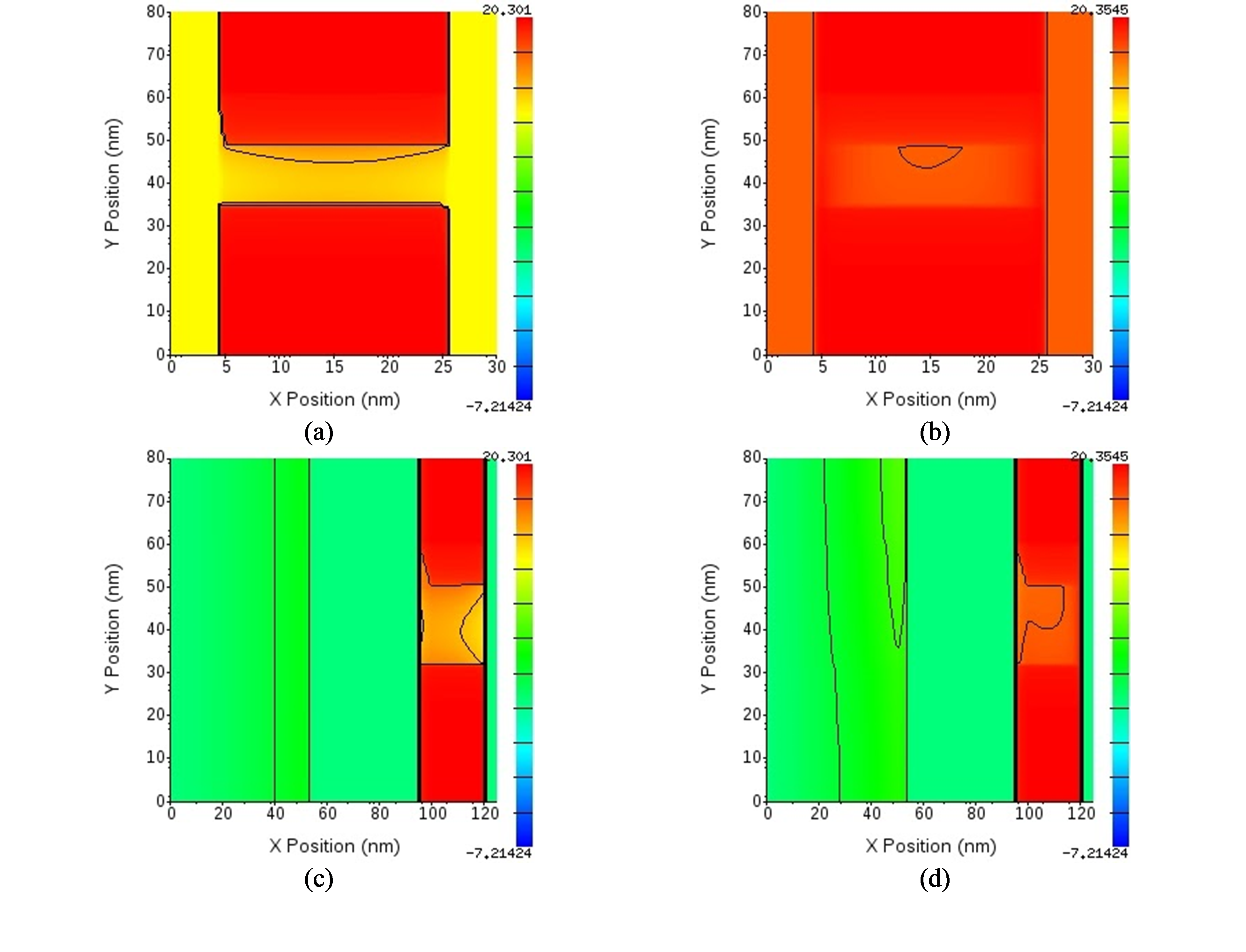
Downloads
References
International technology roadmap for semiconductors, Available at: http://www.itrs2.net, accessed July 2020.
A Balhara and D Punia. Design and analysis of double gate MOSFET devices using High-k dielectric. Int. J. Electr. Eng. 2014; 7, 53-60.
T Skotnicki, JA Hutchby, TJ King, HSP Wong and F Boeu. The end of CMOS Scaling: Toward the
introduction of new materials and structural changes to improve MOSFET performance. IEEE Circ. Devices Mag. 2005; 21, 16-26.
JA Hutchby, GI Bourianoff, VV Zhirnov and JE Brewer. Extending the road beyond CMOS. IEEE Circ. Dev. Mag. 2002; 18, 28-41.
R Compano. Technology roadmap for nanoelectronics. 2th ed. European Commission, Brussels, Belgium, 2000.
Balestra, F Cristoloveanu, S Benachir, M Bimi and J Elewa. Double gate silicon-on insulator transistor with volume inversion: A new device with greatly enhanced performance. IEEE Electron Dev. Lett.1987; 8, 410-2.
RH Yan, A Ourmazd and KF Lee. Scaling the Si MOSFET: From Bulk to SOI to Bulk. IEEE Trans. Electron Dev. 1992; 39, 1704-10.
S Devi, A Singh, R Lorenzo and S Chaudhury. Comparative study of single gate and double gate fully depleted silicon on insulator MOSFET. In: Proceedings of the 2015 International Conference on Communication, Control and Intelligent Systems, Mathura, India. 2015.
J Saint-Martin, A Bournel and P Dollfus. Comparison of multiple-gate MOSFET architectures using Monte Carlo simulation. Solid State Electron 2006; 50, 94-101
GSM Galadanci, A Tijjani and SM Gana. Performance analysis of electrical characteristics of single gate and double gate nano-MOSFET devices. Am. J. Eng. Res. 2018; 7, 248-59
MNIA Aziz, F Salehuddin, ASM Zain, KE Kaharudin and SA Radzi. Comparison of electrical characteristics between Bulk MOSFET and silicon-on-insulator (SOI) MOSFET. J. Telecomm. Electron. Comput. Eng. 2014; 6, 45-9.
R Prasher, D Dass and R Vaid. Performance of a double gate nanoscale MOSFET (DG-MOSFET) based on novel channel materials. J. Nano Electron. Phys. 2013; 5, 01017.
S Jabeen, S Jha and P Anuradha. Impact of variation of device parameters on the electrical characteristics of double-gate Mosfets. Int. J. Innovat. Tech. Explor. Eng. 2020; 9, 2278-3075.
A Lakhanpal, SB Rana, AK Rana. Performance Analysis of Graded Channel Double-Gate MOSFET in Nano-Regime using TCAD Simulation. Int. J. Comput. Appl. 2017.
JK Saha, N Chakma and M Hasan. Impact of scaling channel length on the performances of nanoscale FETs. In: Proceedings of the 9th International Conference on Electrical and Computer Engineering, Dhaka, Bangladesh. 2016.
R Singh. Partially and fully depleted SOI MOSFET’s. Department of Electrical Engineering, IIT Kanpur, Kanpur, India, 2014.
A Wagadre and S Mane. Design & performance analysis of DG-MOSFET for reduction of short channel effect over Bulk MOSFET at 20 nm. Ankita Wagadre Int. J. Eng. Res. Appl. 2014; 4, 30-4
SK Gupta, A Baidya and S Baishya. Simulation and analysis of gate engineered triple metal double gate (TM-DG) MOSFET for diminished short channel effects. Int. J. Adv. Sci. Tech. 2012; 38, 15-24.
PM Zeitzoff and HR Huff. MOSFET Scaling trends, challenges, and key associated metrology issues through the end of the roadmap. AIP Conf. Proc. 2005; 788, 203.
SS Ahmed, SR Mehrotra, S Kim, M Mannino, G Klimeck, D Vasileska, X Wang, H Pal and G Wahyu. Simulates the current-voltage characteristics for bulk, SOI, and double-gate field effect transistors (FETs), Available at: https://nanohub.org/resources/mosfet, accessed December 2017.
J Jose, A Ravindran and KK Nair. Study of temperature dependency on MOSFET parameter using MATLAB. Int. Res. J. Eng. Tech. 2016; 3, 1530-3.
Downloads
Published
How to Cite
Issue
Section
License

This work is licensed under a Creative Commons Attribution-NonCommercial-NoDerivatives 4.0 International License.