
Neutron Radiation Effects on the Performance of the CdSe Thin Film for Photodetector Applications
DOI:
https://doi.org/10.48048/tis.2024.8541Keywords:
CdSe, PLD, Neutron flux, Responsivity, Thin film, Dark current, Crystallite size, Nd: YAG laserAbstract
Cadmium Selenide CdSe thin films were deposited on (7.5×1.3×0.1 cm3) glass substrates and (1×1 cm2) p-type silicon substrates using pulsed laser deposition technique (Nd: YAG laser beam with 80 mJ energy, λ = 1064 nm). Then, they were annealed at 300 °C for 1 h to get diodes as visible light detectors. Some of these samples (diodes) were exposed to different intervals (5, 7, 9, 12) days of neutron radiation using (241Am -10Be) source with a flux of 3×10⁵ n/cm2.s and energy of 5.71 MeV. For comparison purposes, the other diodes were kept without any irradiation The morphological and electrical properties of these samples were studied by XRD, FE-SEM and I-V measurements. Results have shown all these thin films exhibit a hexagonal structure. However, there is a slight shift in the preferred orientation (100) for the irradiated films. Also, there was a new (102 - SiO2) peak that appeared in the irradiated thin film pattern. The crystallite size of pristine and (5, 7, 9, 12) days irradiated CdSe thin films were (26.9, 18.3, 24.9, 20.3 and 24.5) nm respectively, whereas, the mean particle size of the pristine film was 37 nm whereas for the irradiated films 53, 64, 73 and 92 nm. Results also show that the band gap of these samples increased from 2.17 eV for pristine thin films to 2.3, 2.48, 2.25, and 2.3 eV for the irradiated thin films. On the other hand, the results of I-V characteristics show the dark/light current. The current under illumination increases when exposed to small values of neutron radiation then it decreases with higher values of exposure. In contrast, the dark current decreases significantly with the irradiation. The effect of the irradiation was clear on the response/recovery period for all devices. Nevertheless, it was more profound in the response/recovery time of pristine devices. Also, the photo-responsivity of the pristine device was larger than the other devices and it was decreased with increasing absorbed doses.
HIGHLIGHTS
- Hexagonal Structure: All CdSe thin films (both pristine and irradiated) exhibit a hexagonal structure, with a slight shift in orientation due to neutron irradiation.
- Neutron Radiation Impact: Neutron radiation causes a significant shift in crystallite size, decreasing the size for irradiated films. Additionally, a new (102 SiO2) peak emerges in irradiated samples, indicating radiation-induced changes.
- Band Gap Increase: The optical band gap of the CdSe films increased with neutron irradiation, starting from 2.17 eV in pristine films to values as high as 2.48 eV after irradiation.
- Morphological Changes: Irradiated films showed increased grain sizes, with neutron exposure leading to the enlargement of mean particle sizes from 37 nm in pristine samples to 92 nm in the most heavily irradiated samples.
- Electrical Behavior: Neutron irradiation impacted the photodetectors' electrical properties. The light current initially increased with small neutron doses but decreased with higher doses, while dark current consistently decreased after irradiation.
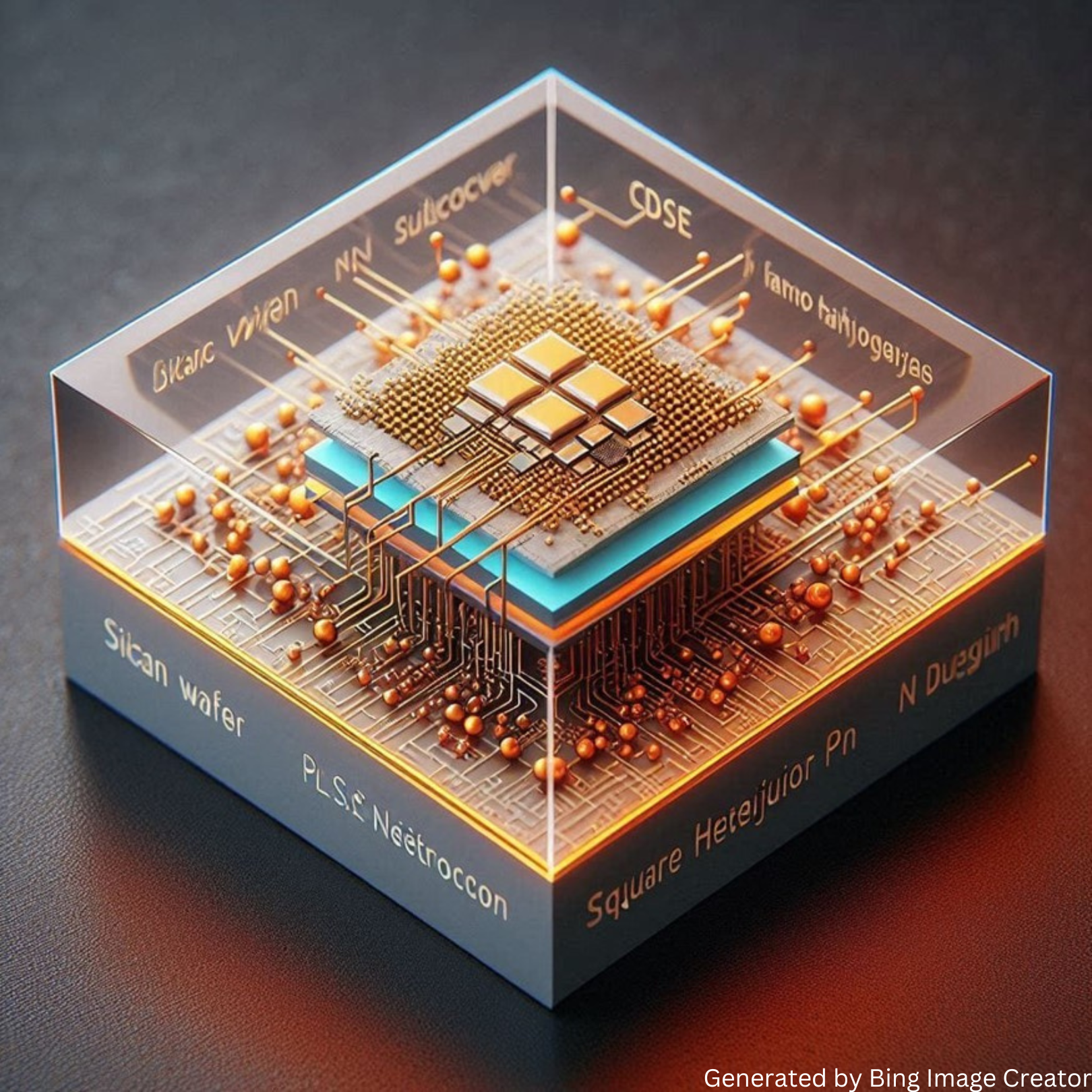
GRAPHICAL ABSTRACT
Downloads
References
MBA Bashir, EY Salih, AH Rajpar, G Bahmanrokh and MFM Sabri. The impact of laser energy on the photoresponsive characteristics of CdO/Si visible light photodetector. J. Micromech. Microeng. 2022; 32, 085006.
RA Soref. Silicon-based optoelectronics. In: Proceedings of the IEEE, New York. 1993. p. 1687-706.
AA Yadav, MA Barote and EU Masumdar. Studies on cadmium selenide (CdSe) thin films deposited by spray pyrolysis. Mater. Chem. Phys. 2010; 121, 53-7.
HH Abed, HM Abduljalil and MA Abdulsattar. Structural, optical and humidity sensitivity for CdSe nanocrystalline thin films. J. Adv. Pharm. Educ. Res. 2018; 8, 25-31.
NT Shelke, SC Karle and BR Karche. Photoresponse properties of CdSe thin film photodetector. J. Mater. Sci. Mater. Electron. 2020; 31, 15061-9.
I Feraru, CR Iordanescu, M Elisa, C Vasiliu, A Volceanov, S Stoleriu, A Peretz and M Filipescu. CdSe-doped phosphate glassy films obtained by PLD on a silicon substrate. Chalcogenide Lett. 2013; 10, 509-17.
G Perna, V Capozzi and M Ambrico. Structural properties and photoluminescence study of CdSe/Si epilayers deposited by laser ablation. J. Appl. Phys. 1998; 83, 3337-44.
RB Konda, R Mundle, H Mustafa, O Bamiduro, AK Pradhan, UN Roy, Y Cui and A Burger. Surface plasmon excitation via Au nanoparticles in n-CdSe∕ p-Si heterojunction diodes. Appl. Phys. Lett. 2007; 91, 191111.
R Choudhary and RP Chauhan. Gamma irradiation induced modifications in spin-coated CdSe thin films. J. Mater. Sci. Mater. Electron. 2016; 27, 11674-81.
P Kumara, D Kumara, A Kumar and RS Katiyarc. Effect of post growth annealing process on optical properties of CdSe thin films on Si p-type substrate deposited by pulsed laser deposition technique. Int. J. Anal. Exp. Modal Anal. 2021; 13, 3016-28.
M Ashry and S Fares. Radiation effect on the optical and electrical properties of CdSe (In)/p-Si heterojunction photovoltaic solar cells. J. Semicond. 2012; 33, 102001.
MA Hernandez-Perez, JR Aguilar-Hernandez, JR Vargas-Garcia, GS Contreras-Puente, E Rangel-Salinas, F Hernandez-Santiago and M Vargas-Ramirez. Influence of the fluence and substrate temperature on the structural and optical properties of CdSe thin films prepared by Pulsed Laser Deposition. Mater. Sci. Forum 2011; 691, 134-8.
MA Hernandez-Perez, J Aguilar-Hernandez, G Contreras-Puente, JR Vargas-Garcia and E Rangel-Salinas. Comparative optical and structural studies of CdSe films grown by chemical bath deposition and pulsed laser deposition. Phys. E Low Dimens. Syst. Nanostruct. 2008; 40, 2535-9.
EY Salih, MBA Bashir, AH Rajpar, IA Badruddin and G Bahmanrokh. Rapid fabrication of NiO/porous Si film for ultra-violate photodetector: The effect of laser energy. Microelectron. Eng. 2022; 258, 111758.
Z Bao, X Yang, B Li, R Luo, B Liu, P Tang, J Zhang, L Wu, W Li and L Feng. The study of CdSe thin film prepared by pulsed laser deposition for CdSe/CdTe solar cell. J. Mater. Sci. Mater. Electron. 2016; 27, 7233-9.
DHA Refaei, LA Najam and LMA Taan. The Effect of neutron irradiation on optical, structural and morphological properties of cadmium selenide thin films. J. Rad. Nucl. Appl. 2021; 6, 207-16.
M Kumari, P Rana and RP Chauhan. Modifications in structural and electrical properties of gamma irradiated CdSe nanowires. Nucl. Instrum. Methods Phys. Res. Section A 2014; 753, 116-20.
M Kaleli, SA Ali, M Koc, S Akyurekli and CA Yavru. Studying the effects of thermal neutrons irradiation on CuInGaSe2 thin film. JMAUC 2020; 12, 186-97.
Z Hammo, L Najam and L Al-Taan. Gamma radiation effects on the performance of the CdSe thin film for photodetector application. Int. J. Eng. Appl. Phys. 2024; 4, 977-83.
EM Noori. Irradiation effect in CdSe thin films. J. Coll. Educ. 2019; 1, 69-76.
C Narula and RP Chauhan. High dose gamma ray exposure effect on the properties of CdSe nanowires. Radiat. Phys. Chem. 2018; 144, 405-12.
TH Mahmoud. Study the effect of thickness on the structural and optical constant of CdSe thin films. J. Coll. Educ. 2017; 18, 249-64.
H Metin, S Erat, ME Ari and M Bozoklu. Characterization of CdSe films prepared by chemical bath deposition method. J. Optoelectron. Adv. Mater. 2008; 2, 92-8.
LA Najam, LMA Taan and DHA Refaei. Preparation and study of the physical properties of CdSe films deposited by a chemical bath method and exposed to neutron irradiation: Effect of neutron Irradiation on a CdSe film prepared. Int. J. Eng. Appl. Phys. 2023; 4, 909-18.
Downloads
Published
How to Cite
Issue
Section
License
Copyright (c) 2024 Walailak University

This work is licensed under a Creative Commons Attribution-NonCommercial-NoDerivatives 4.0 International License.