
Effect of Intensity and Wavelength of Illumination on the Photoelectronic Properties of Nanocrystalline CdSe Thin Films
DOI:
https://doi.org/10.48048/tis.2023.3530Keywords:
Decay time, Molarity, Nanocrystalline CdSe thin films, Photocurrent, Trap levelAbstract
Photoelectronic properties of nanocrystalline CdSethin films prepared by chemical bath deposition (CBD) technique at room temperature are studied taking its molar concentration as a function. Structural analysis of the deposited thin films shows that change of molarity brings a variation in the crystalline sizes of the thin films. Such thin films show suitable photoelectronic properties for the construction of different optoelectronic devices. The photocurrents are observed to be significantly defect controlled in the visible range of wavelengths. The transport mechanism for the thin films is generally a doubly activated process and the photocurrent decay characteristics curves are found to exhibit 2 different decay times which actually correspond to 2 distinct trap levels.
HIGHLIGHTS
- The photoelectronic properties of nanocrystalline CdSe thin films deposited by CBD method are studied
- From the XRD of the films diffraction peaks may be indexed to diffraction basically from the (111) plane of zincblende structure
- The optical band gap may be varied with the molarity of the solution used for deposition
- Photoelectronic properties are dependent of the intensity of different monochromatic illuminations
- Photocurrents for the films are basically controlled by the grain boundary defects
- Growth and decay of photocurrent are effectively governed by different kind of traps
GRAPHICAL ABSTRACT 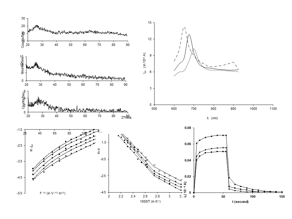
Downloads
References
PK Sahu, R Das and R Lalwani. Incorporation of tin in nanocrystalline CdSe thin films: A detailed study of optoelectronic and microstructural properties. Appl. Phys. Mater. Sci. Process. 2018; 124, 665.
S Hussain, M Iqbal, AA Khan, MN Khan, G Mehboob, S Ajmal, JM Ashfaq, G Mehboob, MS Ahmed, SN Khisro, CJ Li, R Chikwenze and S Ezugwu. Fabrication of nanostructured cadmium selenide thin films for optoelectronics applications. Front. Chem. 2021; 9, 661723.
NT Shelke, SC Karle and BR Karch. Photoresponse properties of CdSe thin film photodetector. J. Mater. Sci. Mater. Electron. 2020; 31, 15061-9.
PKSahu and R Das. Influence of trivalent bismuth doping on optoelectronic and microstructural properties of hydrophilic nanocrystalline cadmium selenide thin films. Thin Solid Films 2020; 693, 137675.
SA Gawali and CH Bhosale. Structural and optical properties of nanocrystalline CdSe and Al:CdSe thin films for photoelectrochemical application. Mater Chem. Phys. 2011; 129, 751-5.
D Nesheva, Z Aneva, S Reynolds, C Main and AG Fitzgerald. Preparation of micro and nanocrystalline CdSe and CdS thin films suitable for sensor applications. J. Optoelectron. Adv. Mater. 2006; 8, 2120-5.
WS Lee, YG Kang, HK Woo, J Ahn, H Kim, D Kim, S Jeon, MJ Han, J Choi and SJ Oh. Designing high-performance CdSe nanocrystal thin-film transistors based on solution process of simultaneous ligand exchange, trap passivation, and doping. Chem. Mater. 2019; 31, 9389-99.
S Nizamoglu, T Ozel, E Sari and HV Demir. White light generation using CdSe/ZnS core-shell nanocrystals hybridized with InGaN/GaN light emitting diodes. Nanotechonology 2007; 18, 065709.
S Mathuri, K Ramamurthi and RR Babu. Effect of Sb incorporation on the structural, optical, morphological and electrical properties of CdSe thin films deposited by electron beam evaporation technique. Thin Solid Films 2018; 660, 23-30.
HN Rosly, KS Rahman, MN Harifand and C Doroody. Annealing temperature assisted microstructural and optoelectrical properties of CdSe thin film grown by RF magnetron sputtering. Superlattice. Microst. 2020; 148, 106716.
Y Yang, T Guo, D Wang, X Xiong and B Li. Preparation and characterization of pulsed laser deposited CdSe window layer for Sb2Se3 thin film solar cell. J. Mater. Sci. Mater. Electron. 2020; 31, 13947-56.
W Pan, J Liu, Z Zhang, R Gu, A Suvorova, S Gain, H Wang, Z Li, L Fu, L Faraone and W Lei. Large area van der Waals epitaxy for II-VI CdSe thin films for flexible optoelectronics and full-color imaging. Nano Res. 2022; 15, 368-76.
M Hassen, R Riahi, F Laatar and H Ezzaouia. Optical and surface properties of CdSe thin films prepared by sol-gel spin coating method. Surface. Interfac. 2020; 18, 100408.
RC houdhary and RP Chauhan. Nitrogen ion implantation effects on the structural, optical and electrical properties of CdSe thin film. J. Mater. Sci. Mater. Electron. 2018; 25, 12595-602.
MS Deora and SK Sharma. Effect of incorporation of sulphur on the structural, morphological and optical studies of CdSe thin films deposited by solution processed spin coating technique. Thin Solid Films 2019; 670, 68-75.
A Alasvand and H Kafashan. Comprehensive physical studies on nanostructured Zn doped CdSe thin films. J. Alloy. Comp. 2019; 789, 108-18.
AM Abdulwahab, AA AL-Adhreai and AAA Ahmed. Influence of Ni-Co dual doping on structural and optical properties of CdSe thin films prepared by chemical bath deposition method. Optik 2021; 236, 166659.
PK Sahu, R Das and R Lalwani. Preparation of nanocrystalline Mg doped CdSe thin films and their optical, photoluminescence, electrical and structural characterization. J. Mater. Sci. Mater. Electron. 2017; 28, 18296-306.
AG Habte, FG Hone and FB Dejene. The influence of malonic acid on the structural, morphological and optical properties of CdSe thin films prepared by chemical bath deposition method. Inorg. Chem. Comm. 2019; 103, 107-12.
SK Tripathi, AS Al-Kabbi, K Sharma and GSS Saini. Mobility lifetime product in doped and undoped nanocrystalline CdSe. Thin Solid Films 2013; 548, 406-10.
K Sarmah and R Sarma. Mobility activation in thermally deposited CdSe thin films. Bull. Mater. Sci. 2009; 32, 369-73.
K Sarmah, R Sarma and HL Das. Effect of wavelength and intensity of illumination on the photoelectronic properties of CdSe thin films. Indian J. Phys. 2008; 82, 585-94.
MN Borah, BJ Baruah, S Chaliha, DP Gogoi, U Mcfarlane and S Dutta. Structural analysis of chemically deposited nanocrystalline CdSe films. J. Exp. Nanosci. 2012; 8, 1-7.
MN Borah and S Chaliha. Characterization of chemically deposited nanocrystalline CdSe thin films from transmittance spectra. Mater. Today Proc. 2021; 46, 5777-80.
LI Maissel and R Glang. Hand book of thin film technology. McGraw Hill Book, New York, 1970.
Joint Committee on Powder Diffraction Standards. Set 20 powder diffraction file. Anal. Chem. 1970; 42, 81A.
A Goswami. Thin film fundamentals. New Age International, New Delhi, 1996.
R Devi, P Purkayastha, PK Kalita, R Sarma, HL Das and BK Sarma. Photoelectric properties of CdS thin film prepared by chemical bath deposition. Indian J. Pure Appl. Phys. 2007; 45, 624-7.
MK Khalaf, BAM ALhilli, AI Khudiar and AA Alzahra. Influence of nanocrystalline size on optical band gap in CdSe thin films prepared by DC sputtering. Photon. Nanostructures Fund. Appl. 2016; 18, 59-66.
R Devi, P Purkayastha, PK Kalita and BK Sarma. Synthesis of nanocrystalline CdS thin films in PVA matrix. Bull. Mater. Sci. 2007; 30, 123-8.
C Mehta, JM Abbas, GSS Saini and SK Tripathi. Electrical and optical properties of n-CdSe. J. Optoelectronics Adv. Mater. 2008; 10, 2461-5.
RB Kale, SD Sartale, BK Chougule and CD Lokhande. Growth and characterization of nanocrystalline CdSe thin films deposited by the successive ionic layer adsorption and reaction method. Semicond. Sci. Tech. 2004; 19, 980-6.
PP Hankare, SD Delekar, PA Chate, SD Sabane, KM Garadkar and VM Bhuse. A novel route to synthesize Cd1-xPb xSe thin films from solution phase. Semicond. Sci. Tech. 2005; 20, 257-64.
J Sharma, R Singh, A Kumar, T Singh, P Agrawal and A Thakur. Size-controlled synthesis of nanocrystalline CdSe thin films by inert gas condensation. Appl. Nanosci. 2018; 8, 359-67.
RH Bube. Photoconductivity in solids. John Wiley and Sons,New York, 1960.
SS Devlin. Physics and chemistry of II-VI compounds. In: M Aven and J Prener (Eds.). North Holand Publishing Company, Amsterdam, Netherlands, 1967.
PK Kalita, BK Sarma and HL Das. Space charge limited conduction in CdSe thin films. Bull. Mater Sci. 2003, 26, 613-7.

Downloads
Published
How to Cite
Issue
Section
License
Copyright (c) 2022 Walailak University

This work is licensed under a Creative Commons Attribution-NonCommercial-NoDerivatives 4.0 International License.